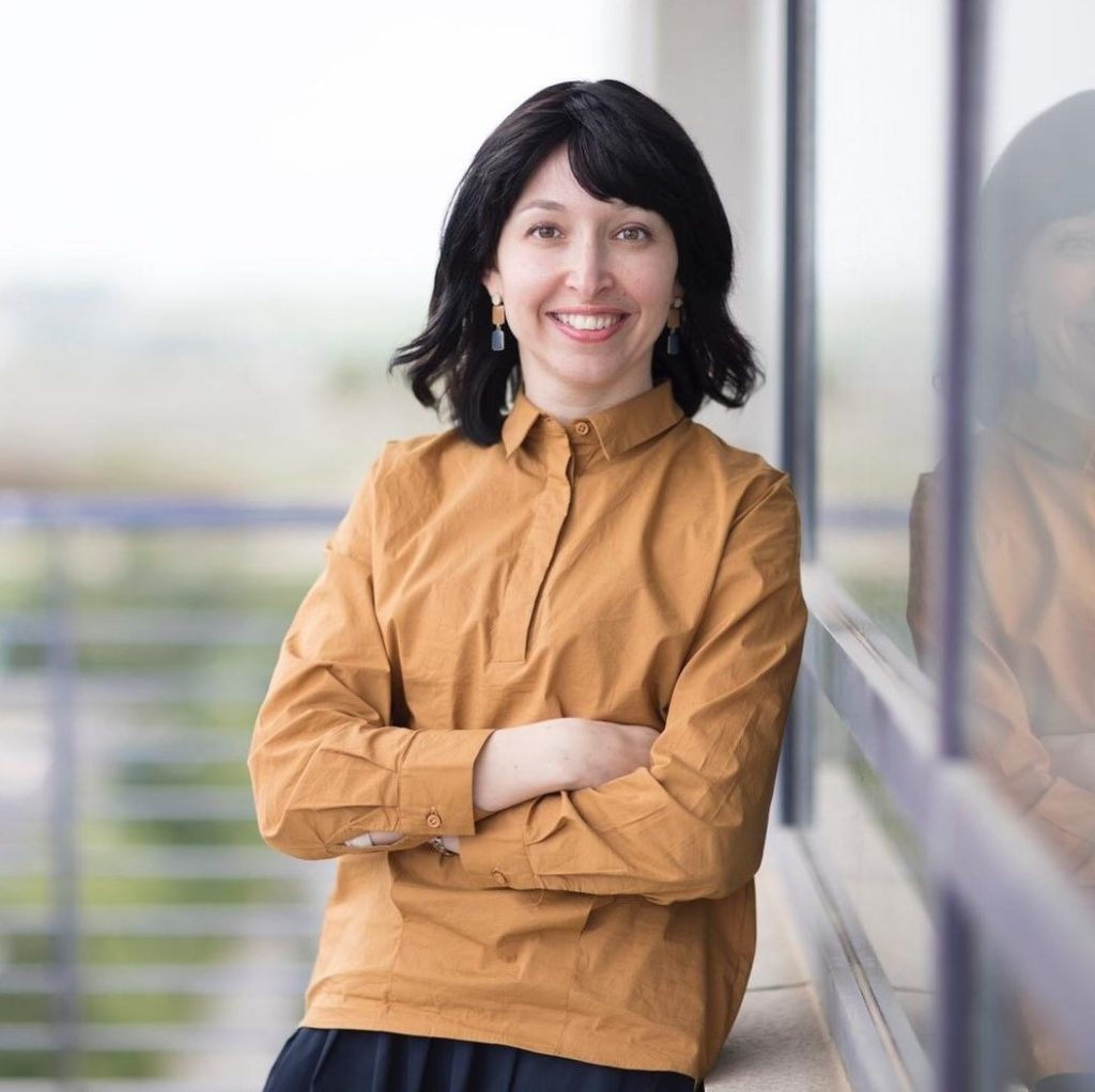

Dr. Anna Levant is an algorithm group manager at Applied Materials. She holds a PhD from Weizmann Institute of Science in Applied Mathematics, specializing in Chaos Problems, and holds numerous patents. Prior to joining Applied Materials, Dr. Levant worked for more than a decade spearheading the development of algorithms for modalities such as MRI, X-ray, and ECG for leading med-tech companies. Dr. Levant promotes women in STEM by teaching Machine Learning and Computer Vision at Haredi women colleges.
Dr. Anna Levant is an algorithm group manager at Applied Materials. She holds a PhD from Weizmann Institute of Science in Applied Mathematics, specializing in Chaos Problems, and holds numerous patents. Prior to joining Applied Materials, Dr. Levant worked for more than a decade spearheading the development of algorithms for modalities such as MRI, X-ray, and ECG for leading med-tech companies. Dr. Levant promotes women in STEM by teaching Machine Learning and Computer Vision at Haredi women colleges.
Sub-nanometer 3D metrology is a fascinating emerging field for the semiconductor industry. As the shrinkage of wafers has reached its physical limit, advanced nodes are resorting to 3D design to increase devices’ feature density. Reliable measurements of these sub-nanometer 3D structures are crucial for the development of innovative chips that support the exponential growth of the technology ecosystem.
Here, we propose a novel supervised ML-based solution for inferring 3D structures from 2D Scanning Electron Microscope (SEM) images, researched and developed at Applied Materials, the leader in chip manufacturing process control. Our algorithm reached sub-nanometer accuracy and high precision, extrapolating the measurements of an unseen 3D structure with an accuracy of ~ 1nm from a single 2D SEM image — even in the presence of shallow and noisy reference data.
Our talk will demonstrate our novel AI-based approach to extracting hidden information from SEM images. We will discuss the generality of the proposed method, and how it opens the door to a plethora of applications in 3D metrology for memory and logic devices.
| 8:45 | Reception |
|---|---|
| 9:30 | Opening words by WiDS TLV ambassadors Or Basson and Noah Eyal Altman |
| 9:40 | Dr. Kira Radinski - Learning to predict the future of healthcare |
| 10:10 | Prof. Yonina Eldar - Model-Based Deep Learning: Applications to Imaging and Communications |
| 10:40 | Break |
| 10:50 | Lightning talks |
| 12:20 | Lunch & Poster session |
|---|---|
| 13:20 | Roundtable session & Poster session |
| 14:05 | Roundtable closure |
| 14:20 | Break |
| 14:30 | Dr. Anna Levant - 3D Metrology: Seeing the Unseen |
| 15:00 | Aviv Ben-Arie - Counterfactual Explanations: The Future of Explainable AI? |
| 15:30 | Closing remarks |
| 15:40 | End |
© 2018-2022 WiDS TLV – Intuit. All rights reserved.
Scotty – By Nir Azoulay
Design: Sharon Geva